SK hynix vs Samsung vs Micron… HBM4 Supremacy Hinges on Packaging and …
 Global competition for HBM4 leadership is intensifying among SK hynix, Samsung Electronics, and Micron. / Image generated by Gemini
The global AI memory market is heating up rapidly. As competition for fourth-generation High Bandwidth Memory (HBM — a memory technology that vertically stacks multiple DRAM chips to enable ultra-fast data transfer) accelerates, the three-way rivalry among SK hynix, Samsung Electronics, and Micron is solidifying. With explosive demand expected for NVIDIA’s next-generation GPU “Rubin,” securing a stable supply chain ahead of competitors is set to become the decisive factor.
HBM features a 3D structure that vertically stacks up to 16 layers of DRAM and connects them using TSV (Through Silicon Via — microscopic electrodes that pass through silicon). When combined with a GPU on a silicon interposer (an intermediate substrate connecting chips) using 2.5D packaging (a method placing chips side-by-side for dense interconnection), data travel distance is shortened, significantly increasing bandwidth while reducing power consumption. The existing HBM3E delivers 1,024 I/O (input/output terminals), up to 9.6Gbps per pin, and achieves 1.2TB/s bandwidth. HBM4 doubles I/O to 2,048 and targets speeds of 11.7–13Gbps per pin, with 2.9–3.3TB/s bandwidth per stack.
While the JEDEC standard specifies 8Gbps, major companies are pushing performance beyond 12Gbps. In 12–16 layer stacks (24–48GB capacity), thermal management and yield rates are critical variables. The base die (control chip at the bottom of the stack) is transitioning to TSMC’s 12FFC (12nm-class FinFET process) or 4nm logic process, improving power efficiency by approximately 40%. DRFM (Directed Refresh Management — selectively recharging specific cells to prevent errors) has also been applied to strengthen resistance against RowHammer attacks.
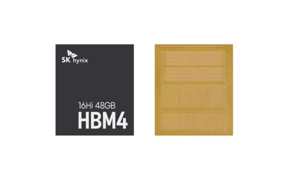
SK hynix announced it has completed HBM4 development first in the world. After its initial announcement in September 2025, the company unveiled a 16-layer 48GB product at CES 2026 in Las Vegas in January 2026, featuring 11.7Gbps, 2,048 I/O, and 2.9TB/s specifications. By combining 1b nm (fifth-generation 10nm-class DRAM process) with TSMC packaging, SK hynix is targeting supply for NVIDIA’s Rubin. Backed by over 60% market share in HBM3E, the company is projected to expand to 70% after mass production begins in the second half of 2026. However, production capacity remains a key variable.
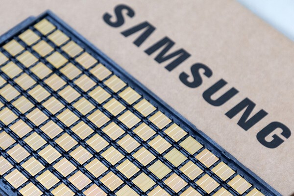
Samsung Electronics has launched a counteroffensive, announcing the industry’s first commercial shipments of HBM4 under a “preemptive shipment” strategy. It supports stable speeds of 11.7Gbps, up to 13Gbps, and 3.3TB/s per stack. Applying a 4nm logic base die reduces power consumption by 40% and improves heat dissipation performance by 30%. The lineup ranges from 12-layer 24–36GB to 16-layer 48GB products. Strengths include customized supply leveraging its foundry operations and dedicated HBM advanced packaging lab, as well as securing NVIDIA certification. Optimization of TSV structure and application of 1c nm (sixth-generation 11nm-class process) DRAM are additional differentiators.
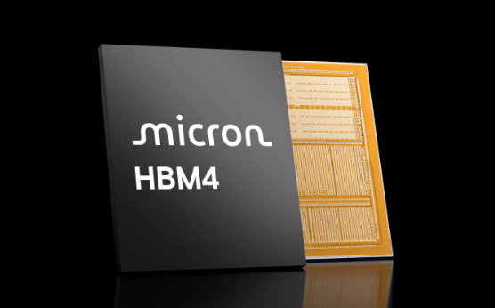
Micron Technology emphasizes efficiency and price competitiveness. After demonstrating power efficiency with its 12-layer HBM3E product, Micron is targeting over 2TB/s bandwidth and speeds exceeding 11Gbps for HBM4. It has established a monthly production capacity of 15,000 wafers and is strengthening cooperation with TSMC to increase U.S.-based production. Although considered slightly behind in high-layer stacking technology, the company aims to capture niche markets through yield stabilization and improved power efficiency. However, in the race to supply NVIDIA, Micron is viewed as being at a relative disadvantage compared with Samsung and SK hynix.
The core of the HBM4 competition lies in detailed technical specifications. As I/O expands to 2,048 bits, PHY (physical layer circuit) area increases to 15㎟ and power consumption rises to 9W. Nevertheless, overall efficiency improves by 1.7 times and area efficiency by 1.8 times. Although NVIDIA Rubin specifications have been raised to above 11Gbps and the mass production schedule has been slightly delayed to late first quarter, market revenue is projected to exceed $20 billion.
Market research firm TrendForce analyzed that NVIDIA is likely to utilize HBM4 products from all three manufacturers to meet massive demand for the Rubin platform. Ultimately, packaging stability and supply capability based on TSMC’s CoWoS (Chip on Wafer on Substrate, advanced 2.5D packaging technology) are expected to determine the winner.

